How China Is Reaching 5nm Without EUV, and How That Impacts ASML

Introduction
It is a common belief that in order for a semiconductor company to manufacture state-of-the-art chips at the 7nm node or lower, EUV (extreme ultraviolet) lithography equipment produced by ASML (ASML) is required, and that less-advanced technology from DUV (deep ultraviolet immersion or ArFi) equipment (also manufactured by ASML and Nikon (NINOY)) was limited to larger dimensions to 10nm.
I wrote in a previous article entitled “Applied Materials: SMIC Move To 7nm Node Capability Another Headwind,” back on May 18, 2022 that China’s main foundry SMIC (Semiconductor Manufacturing International Corporation) had reached the 7nm without EUV, of which EUV equipment had been sanctioned by the U.S. My article didn’t get much attention until it was discovered months later in a teardown that the Huawei Mate 60 Pro smartphone used the Kirin 9000 chip manufactured in China with the 7nm node dimensions.
This week we learned that that Shanghai Microelectronics Equipment (SMEE) had applied for a patent covering an EUV lithography machine on March 2023, reports the South China Morning Post.
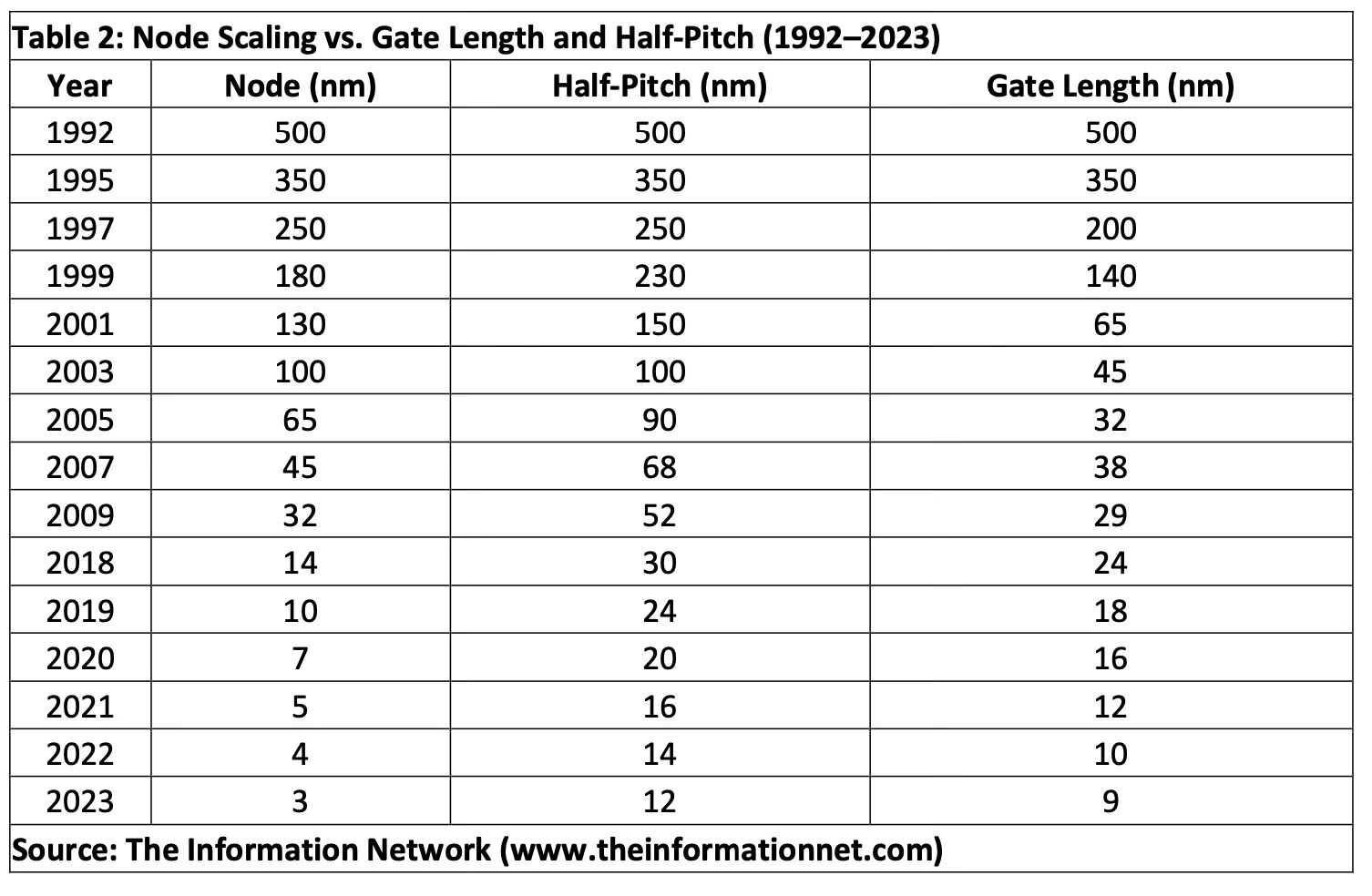
Table 1 shows my analysis of the demand for the various types of lithography systems, according to my report entitled Sub-100nm Lithography: Market Analysis and Strategic Issues on my website. Importantly, ASML is the only company that produces all four types of equipment.
As I said above, EUV is generally required to reach the 7nm node. Importantly, DUV lithography is also required, since not all mask levels use EUV. That mean that even without EUV, ASML stands to benefit from sales of DUV systems, particularly to China, where EUV is sanctioned.in fact in 2024, nearly 50% of ASML’s revenue was generated from China, despite that fact that none of its expensive ($185 million) EUV systems were able to be exported to China.
In this article, I explain how China will be able to be competitive at the 5nm node to those made by TSMC (TSM), Samsung (SSNLF), and Intel (INTC) without EUV, although there are several requisites.
The semiconductor industry’s most advanced chips today are built using extreme ultraviolet (EUV) lithography. TSMC, Samsung, and Intel have incorporated EUV into their 7nm, 5nm, and 3nm production lines, enabling higher density, better power efficiency, and smaller die sizes. However, China’s top foundry, SMIC, lacks access to EUV tools due to export restrictions. Despite this, SMIC is advancing node technologies using only deep ultraviolet (DUV) multi-patterning, pushing toward a 5nm-class node. This article explores how China has reached this point, compares the technological metrics of different nodes, and highlights the trade-offs between DUV and EUV-based approaches.
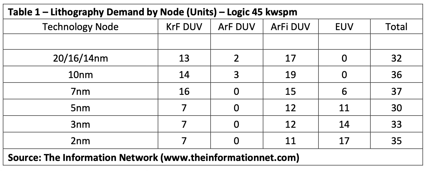
Understanding Historical Node Definitions and Their Drift
As semiconductor scaling has advanced, the definitions of process nodes have become increasingly detached from physical dimensions like gate length and half-pitch. Table 1 traces this evolution, showing how in the early years, node naming aligned closely with physical features. From 14nm onward, the marketing-driven node names no longer match transistor dimensions precisely. This discrepancy is especially important when comparing chips built with different lithographic techniques, such as EUV versus DUV.