
Semiconductor Manufacturing Is Splitting Into Two Worlds

What’s in This Article
Semiconductor Manufacturing Is Splitting Into Two Worlds
Regional Distribution of Global 12-Inch Wafer Fabrication Capacity
Table 1. Regional Distribution of Global 12-Inch Wafer Fabrication Capacity
China’s Mature-Node Manufacturing Expansion
Table 2. Mainland China Wafer Fab Capacity by Wafer Size (2025)
China’s True Share of Global Wafer Manufacturing
Table 3. China Wafer Output Converted to 12-Inch Equivalent Capacity
Investor Takeaway
The global semiconductor manufacturing industry is entering a structural transition that investors have not yet fully recognized. According to SEMI, global 12-inch wafer fabrication capacity is projected to reach approximately 9.6 million wafers per month in 2026, representing an 8 percent compound annual growth rate from 2022 levels. The expansion reflects massive capital spending by the industry’s largest manufacturers—including TSMC, Samsung, Intel, and SMIC—as well as government industrial policy initiatives in the United States, Europe, and China.
The geographic distribution of that capacity expansion is quietly reshaping the balance of power in the semiconductor industry, with implications for supply chains, geopolitical risk, and semiconductor equity valuations.
Behind this growth, however, the geographic structure of semiconductor manufacturing is beginning to diverge into two distinct ecosystems. Advanced logic nodes below roughly 20 nanometers remain concentrated in Taiwan and the United States, dominated by companies such as TSMC, Samsung, and Intel. At the same time, the majority of mature-node semiconductor production—covering analog chips, power devices, microcontrollers, automotive semiconductors, and many industrial components—is rapidly consolidating in mainland China.
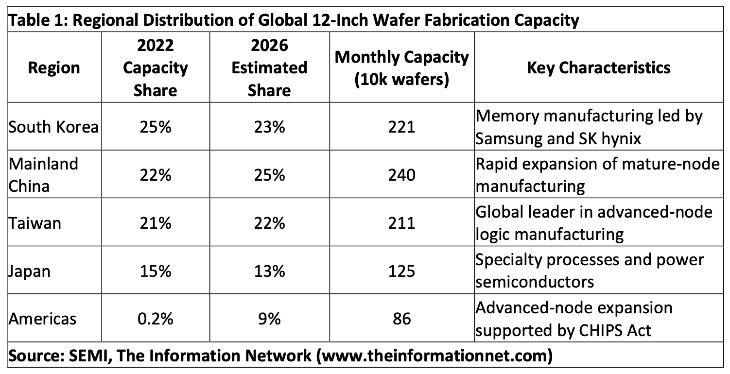
This shift is visible in the regional distribution of global wafer capacity
According to Table 1, mainland China’s share of global 12-inch wafer fabrication capacity is projected to rise to roughly 25 percent by 2026, surpassing both South Korea and Taiwan. The increase reflects a wave of fab construction during the past several years, supported by both domestic semiconductor investment programs and strategic efforts to localize supply chains following U.S. export controls.
South Korea and Taiwan remain major manufacturing centers, but their global share declines slightly as capacity expands in other regions. Korea’s production remains heavily concentrated in memory manufacturing dominated by Samsung and SK hynix, while Taiwan continues to lead the industry in advanced logic nodes through TSMC. Japan maintains a strong position in specialty processes and power semiconductors, while the Americas see the largest percentage increase in capacity as new fabs are built in the United States.
The rise in the Americas—from almost negligible share in 2022 to roughly 9 percent by 2026—is largely attributable to the construction of new facilities by TSMC in Arizona, Samsung in Texas, and Intel’s expansion of domestic manufacturing. These projects represent the most visible outcome of the U.S. CHIPS and Science Act, which aims to restore advanced semiconductor manufacturing capacity within the United States.
China’s Mature-Node Manufacturing Expansion
While the global capacity distribution highlights China’s growing importance, it understates the scale of the country’s manufacturing footprint because it focuses only on 12-inch wafer fabrication. China’s semiconductor ecosystem includes a large number of fabs producing on smaller wafer sizes, which are still widely used in mature-node semiconductor production.
According to Table 2, mainland China currently operates dozens of wafer fabrication facilities across multiple wafer sizes, including 58 twelve-inch fabs, 36 eight-inch fabs, and 48 six-inch fabs. These facilities collectively represent one of the largest semiconductor manufacturing footprints in the world. Data in this article come from my report at The Information Network entitled “Mainland China’s Semiconductor and Equipment Markets: Analysis and Manufacturing Trends.”